(Hong Kong)

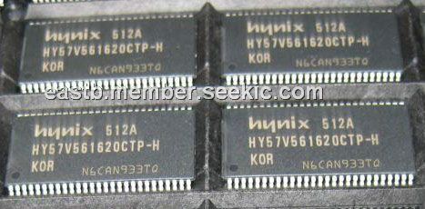
Product Summary
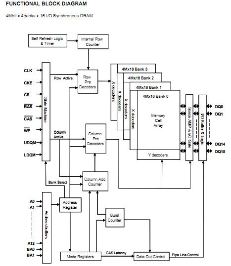
The HY57V561620CTP-H is a 268,435,456bit CMOS Synchronous DRAM, ideally suited for the main memory applications which require large memory density and high bandwidth. The HY57V561620CTP-H is organized as 4banks of 4,194,304x16. The HY57V561620CTP-H is offering fully synchronous operation referenced to a positive edge of the clock. All inputs and outputs are synchronized with the rising edge of the clock input. The HY57V561620CTP-H’data paths are internally pipelined to achieve very high bandwidth. All input and output voltage levels are compatible with LVTTL.
Parametrics
HY57V561620CTP-H absolute maximum ratings: (1)Ambient Temperature, TA: 0 ~ 70 ℃; (2)Storage Temperature, TSTG: -55 ~ 125℃; (3)Voltage on Any Pin relative to VSS, VIN, VOUT: -1.0 ~ 4.6 V; (4)Voltage on VDD relative to VSS, VDD, VDDQ: -1.0 ~ 4.6 V; (5)Short Circuit Output Current, IOS: 50 mA; (6)Power Dissipation, PD: 1W; (7)Soldering Temperature · Time, TSOLDER: 260 · 10℃·Sec.
Features
HY57V561620CTP-H features: (1)Single 3.3±0.3V power supply; (2)All device pins are compatible with LVTTL interface; (3)JEDEC standard 400mil 54pin TSOP-II with 0.8mm of pin pitch (Leaded Package or Lead Free Package); (4)All inputs and outputs referenced to positive edge of system clock; (5)Data mask function by UDQM, LDQM; (6)Internal four banks operation; (7)Auto refresh and self refresh; (8)8192 refresh cycles / 64ms ; (9)Programmable Burst Length and Burst Type: 1, 2, 4, 8 or Full page for Sequential Burst;1, 2, 4 or 8 for Interleave Burst; (10)Programmable CAS Latency ; 2, 3 Clocks.
Diagrams
T") |
 HY57V121620(L)T |
Other |
|
Data Sheet |
Negotiable |
|
||||
|
HY57V161610D |
Other |
|
Data Sheet |
Negotiable |
|
||||
|
HY57V161610D-I |
Other |
|
Data Sheet |
Negotiable |
|
||||
|
HY57V161610E |
Other |
|
Data Sheet |
Negotiable |
|
||||
|
HY57V161610ET-I |
Other |
|
Data Sheet |
Negotiable |
|
||||
|
HY57V161610ETP-I |
Other |
|
Data Sheet |
Negotiable |
|
||||